Maximizing New User Experiences with High Definition,
High Magnification and Ultra-Slim Design
Samsung Electro-Mechanics has high-precision design technology and mass-production technology for actuators,
which are the core components of camera modules. We offer high-end camera modules with various functions
based on high-performance slim actuator technology that can be used with high-resolution lenses.

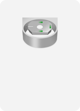
Actuator
An actuator is a component in a camera module that moves the lens up and down or left and right at high speed to focus or stabilize images. Major functions include AF, OIS, iris, and optical zoom.

- AF(Auto-Focus)
- A feature that moves the lens to the optimal focal point for a sharp image of your subject.
- OIS(Optical Image Stabilizer)
- A feature that detects subtle camera shake
and calibrates the lens to the opposite
position of the shake to prevent image blur.
- IRIS
- A feature that adjusts the amount of light
to shoot with optimal lighting and depth.
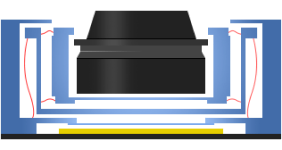
Advanced Ball Guide Actuator
The optimized ball guide method is applied to Samsung Electro-Mechanics actuator products. This enables precise AF and OIS operation of heavy lens components compared to suspension or spring support methods. By applying a 2-axis ball guide by categorizing the support area into X, Y stages during OIS operation, we were able to eliminate the rolling phenomenon by eliminating crosstalk during operation of each axis. It has superior operation speed and positioning accuracy and has strengths in reducing battery consumption as well as high reliability.

- Ball Guide Structure (high reliability, high precision)
- Productivity improvement and failure mode minimization through structural optimization and simplification
- Superior impact resistance reliability compared to alternative methods
- Precision control of OIS & AF through closed-loop control system
- Precision operation of high resolution lens possible in line with high pixel trend
- Low power operation possible with structure optimized for mobile use
| Type | Ball Guide | Spring & Wire |
|---|---|---|
| Structure | 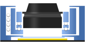 |
 |
| Settling Time | (Relatively) Short | Long |
| Crosstalk | No | Yes |
| Weight Limit | Over 1000mg | Below 1000mg*Spring deformity and wire breakage occurs upon impact |
| Power Consumption | Low | High |
| Compensation Angle | High (1.5˚) | Low (1.0˚) |
* Spring deformity and wire breakage occurs upon impact
Optical Zoom Actuator
Optical zoom is the use of multiple layers of lenses to control different magnification ratios. Unlike the digital zoom, optical zoom allows
you to take bright, sharp photos of distant subjects at high magnification. There are two types of optical zoom: the traditional vertical method,
where the light path is straight, and the folded method, where the light path is bent like a periscope to create a high magnification zoom.
- Slim & high definition folded (refracting optical system applied) and high magnification zoom modules
- Ball guide structure enables the use of heavy weight lenses for big sensors
- Easy to secure high magnification and high resolution with prism OIS + ball guide structure
- Lens optical align assembly ensures high resolution
- Easy to expand performance: Long stroke applied multi-level zoom, super macro, lens lead application possible
- Closed-loop control system ensures high precision
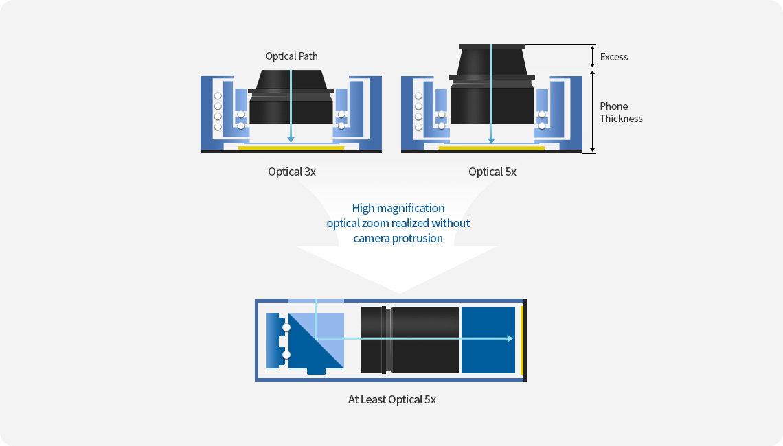
Vertical vs Folded
As a generally-used structure, in order to obtain the high magnification optical zoom for the vertical method, it is necessary to
secure long focus distance, and therefore, the height of the camera module increases and results in a camera design that may
undermine smartphone design. As a result, the camera module with vertical zoom method has limitations in obtaining high magnification
optical zoom and typically can support up to 2-3x optical zoom only. The folded method applies a structure based on the principle of a
periscope, folds light through a prism, and directs the folded light through horizontally aligned lens and sensors. Through this, there is
no need to increase the thickness of the camera module when securing long focus distances, and high optical magnification.
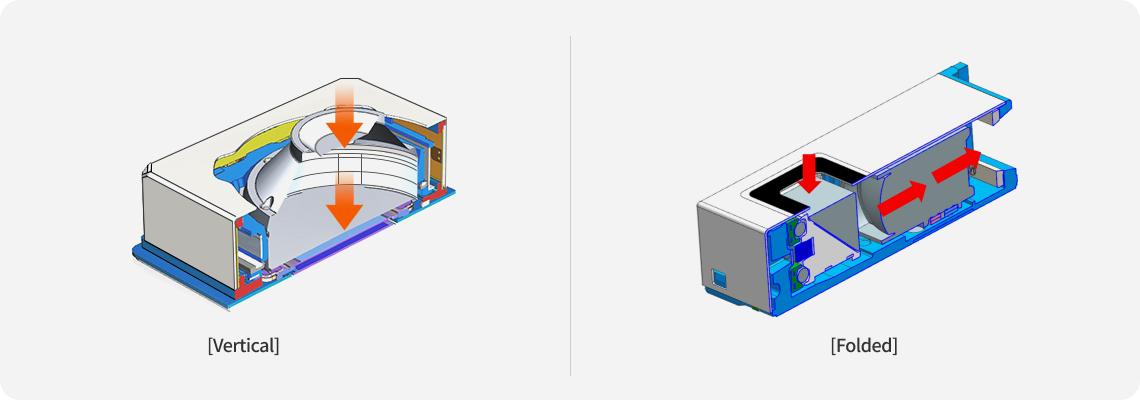
The traditional vertical method of magnification requires the height of the camera module to increase as magnification increases,
even up to such heights that make phone testing impossible at an optical zoom of 5X or more. The folded method allows slim design and
high optical magnification without the protrusion of the camera module in the phone.
Lens
The lens is a component that collects the light emitted from the subject and delivers it to the image sensor to form an image of the subject.
We have secured a diverse product lineup to support wide, telephoto, ultra wide, front, and high magnification zoom camera modules
for mobile use, as well as rear view, surround view, e-mirror, front facing, and interior camera modules for automotive use.
- High resolution slim lens core technology
- Slimmer high-pixel lenses of 48M, 50M, 108M and 200M
- Lens design technology for realizing high resolution
- World’s first mass production of 7p lens
- Precise mold production and assembly technology at sub-micron size
- World’s first mass production of folded camera module with D-cut lens
- Consistent manufacturing system development of optics/optical tool design → mold design/production → lens injection/assembly
* Sub-micron : Diameter 0.2~0.1um, 1um=0.0001cm
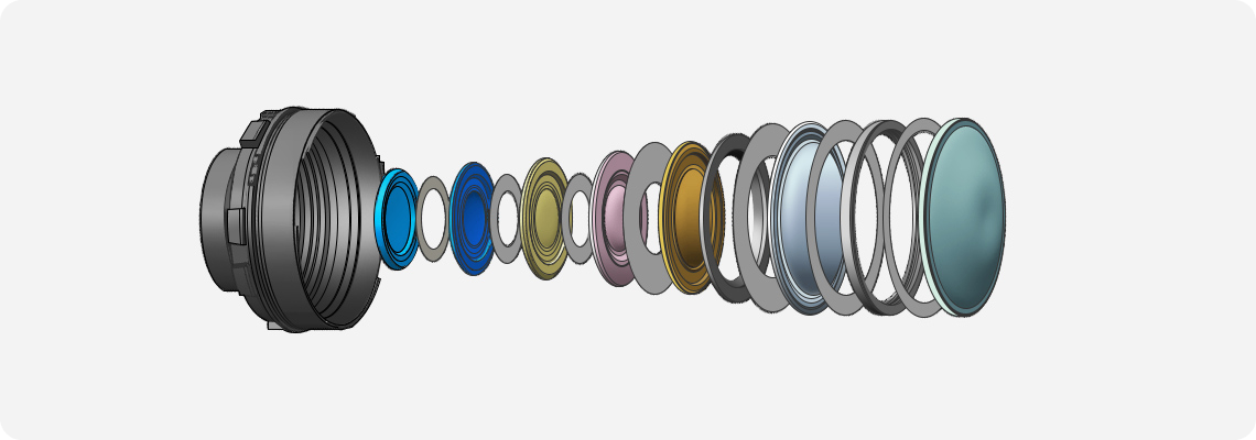
Lens Assembled Products
Lens assembled products are generally comprised of 3 types of components, including barrels, lens, and spacers.
The barrel serves as a case that brings together all lens components, the lens directs light so that the image is formed on the sensor,
and the spacer serves a role in blocking out unnecessary light to prevent flares or ghosts while maintaining a distance between the lens.
* Flare : A phenomenon where the image looks fuzzy as a result of light being reflected within the barrel or the subject being too bright and resulting in a diffused reflection
* Ghost : A phenomenon where an afterimage is left at the location symmetric to the light source due to the reflection of strong light within the barrel or on the lens
Each lens parameter has a direct influence in determining the resolution of the camera module. In order to obtain an exceptional resolution, the following lens parameters are managed at the sub-micron level.
| Lens Measurement Item | Description |
|---|---|
| Decenter | Distance between the centers of both sides of the lens |
| Concentricity | Distance between the center of the external diameter of the lens and center of the effective area of the lens |
| Rib Thickness | Thickness of the rib (external side of the effective lens) |
| SAG | Distance from the rib of the lens (assembly base area) to the inflection point of the lens |
| Central Thickness | Thickness of the lens center |
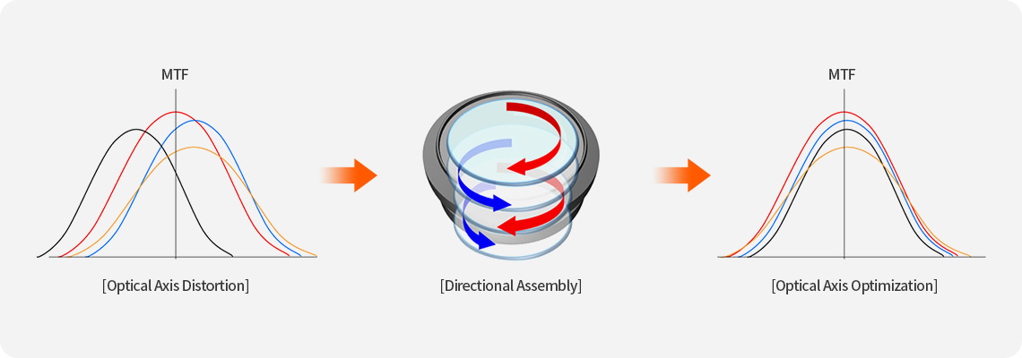
In order to obtain high resolution, the management of lens parameters is important, but it is also important to minimize
the optical axis distortion during the process of assembling each lens component. Through the directional assembly
that involves the rotation and assembly of each lens component, it is possible to align the distorted optical axis to obtain clean images.
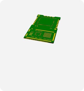
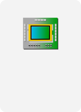
PCB
PCB is comprised of the combination of various materials, including PSR, copper foil, and insulators, then actuators, sensors,
and circuit elements are placed on the PCB to transfer digital images through a circuit between components.
The camera module uses a rigid-flexible PCB mounted by a curved shape in a dense space of electronic products and
a flexible PCB for internal mounting of the camera module actuator.

- PCB design core technology
- Warpage interpretation automation
- PCB thin printing structure (FR-4 0.3T, FR-4 Cavity 0.25T, Metal Cavity 0.15T)
- Electrical simulation
- 3D Warpage Scan
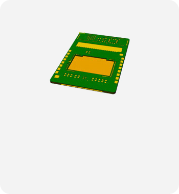
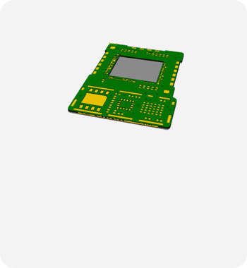
PCB Thin Printing Structure
The technological environment of mobile devices is rapidly progressing towards high performance and slimness, and in order to create
slimmer camera modules, technology to reduce the thickness of components is required. The slimness of the PCB provides
additional slimness to the camera module by using cavity PCB which reduces the thickness of the PCB in the area where the sensor is placed.
-
- FR-4 Normal PCB
- Thickness: 0.3
-
-
Organic Cavity PCB
(Cavity FR-4 Material) - Thickness: 0.4(Cavity 0.2)
-
Organic Cavity PCB
-
-
Metal Cavity PCB
(Cavity Metal Material) - Thickness: 0.4(Cavity 0.15)
-
Metal Cavity PCB
Warpage Interpretation Automation
PCB warpage management is a factor that influences the optical performance of the camera module, and it is a key technology for
high pixel/resolution camera modules. Warpage interpretation, based on the CTE mismatch theory, simulates warpage to provide prediction
with higher accuracy. Using interpretation model, optimization algorithm development, and program development,
we have automated the entire interpretation process. Through this, we obtain the optimal results then apply them to the design.
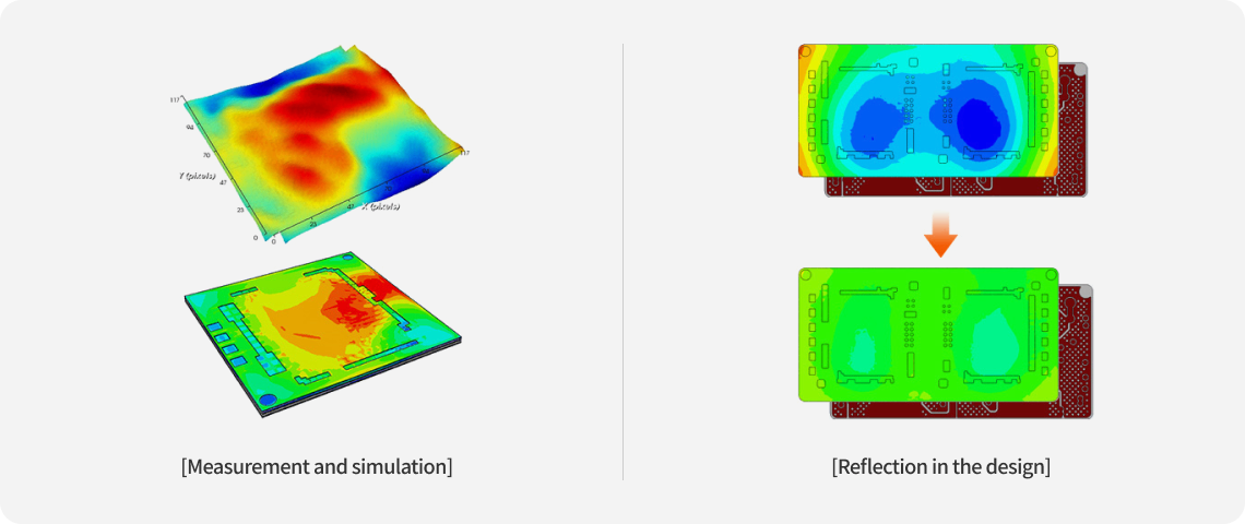
* CTE(Coefficient of Thermal Expansion) : Coefficient of thermal expansion, ratio of thermal expansion and temperature for an object withstanding a certain pressure
Electrical Simulation
With regards to camera module technology progression, high-speed signal transmission and low power are required,
and design that minimizes losses with regards to low power component development and PCB design is required.
Through electrical simulation of transmission lines, such losses can be predicted with greater accuracy,
and design improvement points are continuously reflected.

- Resistance [mΩ] analysis
- Coupling Coefficient [%] analysis
- MIPI Impedance analysis
- S-Parameter Analysis
Module PKG
Through field test, assembly, and inspection/evaluation of optical components, our manufacturing technology provides
optimized camera module performance.
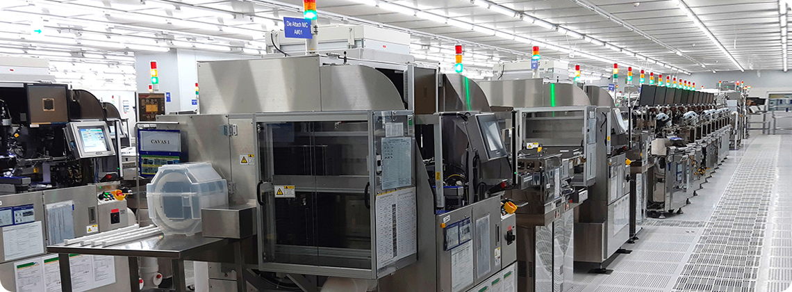
- High productivity with high-speed automation
- Precision assembly process for high quality products (Active Alignment)
- Slim PKG process / technology for ultra-thin products
- Automation of product property evaluation and particle inspection processes (Full Automation)
- In-house development of high-precision process equipment
- Highly clean product manufacturing environment (10class)
COB
COB (Chip on Board) is a packaging method in which image sensors are mounted on a rigid PCB and the PCB and sensor are connected
by wire bonding. It is a method that is widely used in the production of semiconductors and various devices because it enables automation
and product standardization and has excellent reliability. Samsung Electro-Mechanics has developed and applied various methods in-house
to produce the world's best camera modules.

The process order for the COB method.
-
- 1. Die Attach
- Attachment of the
image sensor to the PCB
-

- 2. Wire Bonding
- Connection of wires to allow electrical signals to flow between the image sensor and PCB
-
- 3. Cleaning
- Removal of foreign material
from the PCB
and image sensor
-

- 4. Housing Attach
- Precise assembly of
the lens-attached housing
with the image sensor
(Active Alignment)